Semiconductors
Semiconductors are those materials whose conductivity lies between insulators and conductors. At 0 Kelvin semiconductors behave as insulators but at room temperature some of the valence electrons move towards the conduction band. This is property by which we can distinguish semiconductors from insulators and conductors. For conductors the valence band and conduction band overlaps and for the insulators the energy gap difference is 7eV but for the semiconductors it is approximately 1.107eV. Therefore at room temperature the valence electrons get enough energy to move from valence band to the conduction band.
Types of semiconductors:
There are two types of semiconductors
· Intrinsic semiconductors
· Extrinsic semiconductors
Intrinsic semiconductors:
Intrinsic semiconductors are those semiconductors in which no impurity is added. For example silicon semiconductor containing all the silicon atoms and not even a single impurity is added is intrinsic silicon semiconductor.
In this type of semiconductors all the conductivity is due to the rupturing of covalent bond. In other words due to heating when the covalent bond breaks and move towards the conduction band the valence electrons move towards the conduction band. For a single structure of silicon there is 5x10²²/cm3 and only one of every billion atom is ionized.
Extrinsic semiconductors:
Extrinsic semiconductors are those semiconductors in which impurity is added and this process is called doping.
Types of extrinsic semiconductors:
There are two types of extrinsic semiconductors
· P-type
· N-type
P-type:
P-type semiconductors are that semiconductor in which trivalent impurity is added i.e. the impurity atom belongs to the 3-A group of the periodic table which has three electrons in the last shell. For example aluminum is selected.
It only form bond with the three valence electrons of silicon and three single bonds will be formed. There will be one vacant space named as hole. This hole will also help for the conductivity. An electron from the other silicon atom will come to fill this space and a hole will be generated there. Similarly another electron from any other silicon atom will come to fill this gap and hole will be generated again. In this way this process will continue and the electrons will move towards the conduction band. One thing should be remembered that the electrons and hole move in the opposite directions. During this process temperature (heat) will be provided to the semiconductors for the rupturing (breaking) of covalent bond of silicon to silicon atoms.
Majority charge carriers:
The charge carriers which are in excess are named as majority charge carriers. In p-type material holes will be the minority charge carriers
Minority charge carriers:
The charge carriers which are lesser in amount are called minority charge carriers. In p-type materials electrons are minority charge carriers.
Recombination:
Thermal ionization (ionization by providing heat) results in the formation of free electrons and holes and due to this ionization the number of electrons is equal to the number of holes. These holes and electrons move randomly throughout the silicon lattice and during this process some of the electrons may fill some of the holes. This process is called recombination and due to this processes some if the free electrons and holes may disappear. So the number of holes and the number of free electrons may not remain equal to the free number of electrons. The rate of recombination is directly proportional to the free number of electrons and holes and it depends upon the ionization rate.
N-type semiconductors:
N-type semiconductors are that semiconductor in which a pentavalent impurity is added i.e. the impurity belongs to the 5-A group of the periodic table which has five electrons in the valence shell. For example phosphorus is selected.
Four of the valence electrons of the impurity will form bond with the four valence electrons of the silicon atom and the fifth electron will be free. This fifth electron will move towards the conduction band and form a bound positive ion. Remember that there is a difference between hole and a bound positive ion. In the hole there is a free space for the formation of a single bond but in the bound positive ion all the four electrons are bonded to the silicon and this fifth electron was free and has moved to the conduction band. There is no free space for the formation of any other bond. This fifth electron will towards the conduction band. In the mean while temperature will be provided to the silicon structure due to which rupturing of covalent bond will continue and it will provide free electrons to the conduction band. Meanwhile hole will also be generated and the electrons from the other silicon atoms will come to fill this vacant space. Same process will continue hole will move downward and the electrons will move upward.
Majority charge carriers:
The charge carriers which are in excess are named as majority charge carriers. In n-type material electrons will be the minority charge carriers
Minority charge carriers:
The charge carriers which are lesser in amount are called minority charge carriers. In n-type materials holes are minority charge carriers.
PN junction:
Now we will discuss the formation of a pn-junction. Pn junction is formed by adding trivalent impurity at one side of the silicon structure and a pentavalent impurity at the other side of the pn junction.
Remember that pn junction cannot be formed by joining p-type and n-type semiconductors.
PN junction incase battery is not attached:
When the battery is not attached to the pn junction followings processes can be happen
· Diffusion of charges & formation of depletion region:
· Electric field direction
Diffusion of charges & formation of depletion region:
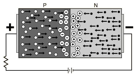
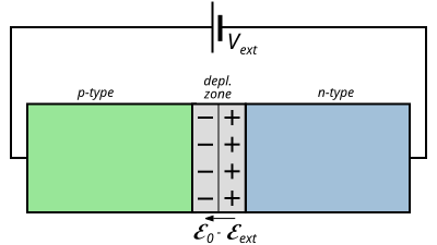
After the formation of pn junction the electrons are in abundance in n-type side and holes are in abundance in p-type. So the electrons of n-type material will diffuse towards the p-type side and combine with the holes and form the neutral atoms. Due to this the number of electrons will decrease in n-side. When the numbers of electrons decrease in the n-side it will give rise to positive charge. Similarly when the electrons combine with the holes it will reduce the number of holes in p-side. Due to decrease of number of holes the negative charge will appear at p-side of the junction. Remember that the positive and negative charges due to the depletion region are different from the holes and electrons of p & n-side of the junction respectively. These positive and negative charges are called mobile ions and they are formed due to the decrease in the number of holes and electrons in the p and n-side of the junction respectively due to the diffusion of charges.
Electric field direction:
You can see in the depletion region the holes (represented with +) are migrated towards n-type region.
And the electrons (represented with -) are migrated towards p-type region. This will produce electric field. In case of silicon the depletion region will be of 0.6 to 0.7V. In case of germanium it will be about 0.2 to 0.3V. The electric field will be directed from positive towards negative as shown in the diagram. This electric field will allow the electrons to move from right to left and holes to move from left to right as electrons flow in the opposite direction of the electric field and holes move in the direction of electric field.
PN junction incase battery is attached:
When the battery is connected to the pn junction then there are two possibilities.
· Forward biased pn junction
· Reverse biased pn junction
Forward biased pn junction:
When the positive terminal of the battery is connected to the p-side of the junction and negative terminal of the battery is connected to the n-side of the junction then it is called forward biased pn junction or forward biased diode.
In the forward biased following things happen.
· Decrease of depletion region
· Drift current
· Diffusion current
Decrease of depletion region:
When the diode is forward the depletion region will decrease. Now it is important to know that how the depletion region will decrease. The negative side of the battery will repel the electrons and the positive side of the battery will repel the holes. When the electrons of the n-type region try to cross the potential barrier (depletion region) they cannot because they don’t have enough energy to cross it. They will combine with the positive mobile ions and neutralize them. Similarly the holes of p- side region will try to cross the potential barrier. In trying to do so the holes will combine with the negative mobile ions and neutralize them. This neutralization will decrease the depletion region and now the holes of the battery can be attracted towards the negative terminal of the battery and the electrons can be attracted towards the positive terminal of the battery.
Diffusion current:
The current which flows due to the majority charge carriers is called diffusion current. In the forward biased pn junction the current flows due to majority charge carriers i.e. in p-type the holes and in n-type the electrons.
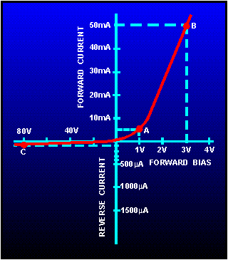
It is the diffusion current in the forward biased pn junction and with a very small change in the voltage we can see a big change in the current. This can be illustrated by the graph given below. You can see in the graph with the increase of roughly 2 volts the current can be increased from 5mA to 50 mA. This increases the importance of the junctions. The resistance is added to limit the current.
Drift current:
Drift current is the current which flows due to minority charge carriers so I will explain it there in the reverse biased pn junction.
Reverse biased pn junction:
When the negative terminal is connected to the p-side of the junction and positive terminal of the battery is connected to the n-side of the junction then it is called reverse biased pn junction.
In the reverse biased pn junction following things can happen
· Increase in the depletion region
· Drift current
· Diffusion current
Increase in the depletion region:
When the junction is in reverse biased condition then the positive side of the battery will attract the electrons towards itself and negative side of the battery will attract the holes towards itself. Due to this the holes and the electrons in their respective areas will decrease and the mobile ions will increase due to which the depletion region will increase. Due to increase in the depletion region the electric field strength will increase and this will support the flow of minority charge carriers.
Drift current:
The flow of electric current due to minority charge carriers is called drift current. In the reverse biased pn junction drift current flows. Because in the p side region there are free electrons but in a very small amount and in the n side region the holes are in a very small amount. These both are called minority charge carriers. The electrons flow in the opposite direction of the electric field and the holes flow in the direction of electric field. The increased electric field will provide the minority charge carriers to flow. The p-type minority charge carriers (electrons) will flow from left to right and the n-type minority charge carriers (holes) will flow from right to left. This current is also called leakage current.
You can see in the negative cycle of the graph that the voltage is continuously increasing but it has no effect on the current and the current is same. Every diode has a limit up to which it can bear the voltage after that the junction break down and this point is commonly known as breakdown point. After the break point the current abruptly increases.
Diffusion current:
Diffusion current is the current which flows due to the majority charge carriers. This will not flow in the reverse biased pn junction.